On August 6, AMD announced it was acquiring Taalas, a three-year-old Toronto startup with 25 engineers and a chip that does something no GPU can: it eliminates the memory bandwidth bottleneck during inference by physically embedding model weights into transistors. The HC1 — Taalas’s first production accelerator — served Meta’s Llama 3.1 8B at 16,960 tokens per second, a number 48 times higher than what Nvidia’s H200 or B200 achieves on the same workload, at a power draw of 200 watts per card. A ten-card server running at 2,500 watts total does what a GPU rack consuming 120 to 600 kilowatts cannot match on token throughput per dollar. That is not an incremental improvement. It is a different class of machine built on a different set of assumptions about what the inference problem actually is.
How You Eliminate a Memory Wall
Every GPU running inference today does the same thing: during each forward pass, the model’s weights are streamed from high-bandwidth memory into on-chip SRAM, multiplied by the input activations, and discarded. For prompt processing — the prefill phase, where the input tokens are encoded in parallel across the full sequence — this is acceptable. The compute intensity is high, parallelism is available, and GPUs are good at parallelized matrix math. But during token generation — the decode phase, where the model produces output one token at a time — the architecture’s weakness becomes the dominant constraint. Each token requires a complete sweep through all the model weights, but produces only a thin slice of new activations. You are running a multi-billion-parameter matrix multiplication to advance the sequence by a single position. The arithmetic intensity plummets. The chip’s compute units sit largely idle while the memory bus works as hard as it can. No amount of additional FLOP capacity fixes this. The bottleneck is memory bandwidth, not compute, and you cannot buy your way out of it with a faster GPU.
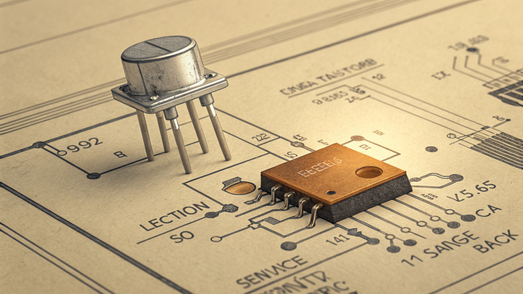
Taalas’s answer was to make the question irrelevant. The company’s Hard Coded Inference architecture, explained in NextPlatform’s February deep-dive, uses a dual-fabric design: a mask ROM recall fabric for model weights, paired with an SRAM recall fabric for the KV cache. The weights do not live in memory. They are the circuit. CEO Ljubisa Bajic described the efficiency at the transistor level: they store four bits and perform the associated multiply operation within a single transistor. Weights and their computations are co-located in the physical device. There is no memory bus for the model parameters, because there is no separation between where the weights live and where the multiplication happens. The HC1 is built on TSMC’s N6 6nm process, contains 53 billion transistors across an 815 square millimeter die, and holds 8 billion parameters — hardwired for one model, one version, permanently. The chip and the model are the same object.
The performance result of this is $0.0075 per million tokens on Llama 3.1 8B, against $0.0379 to $0.286 per million on GPU-based infrastructure. The power gap is comparable: 12 to 15 kilowatts per rack versus 120 to 600 for the GPU equivalent, with the HC1 running at standard air cooling in PCIe card form factor. These are Taalas’s own numbers from controlled benchmarks and should be treated as directionally accurate rather than precise production measurements — batch size, context length, quantization settings, and hardware configuration all affect real-world comparisons. But the gap is large enough that its direction is not in question. The HC1 achieves this partly through aggressive quantization: 3-bit and 6-bit parameters rather than the 16-bit or 8-bit precision most GPU deployments use. That accuracy tradeoff is real, and quality-sensitive inference providers may not accept it. Taalas’s efficiency numbers assume you can live with the quantization. Some workloads cannot.
The Bet Inside the Acquisition
There is an obvious objection to model-specific silicon, and Taalas’s own CEO named it precisely. Speaking to the Turing Post earlier this year, Bajic said: “The big thing at the root of this idea is the assumption that the customer is willing to commit to this chip-model combination for a year.” A GPU deploys new model checkpoints as software updates. Changing the HC1’s weights requires a new tape-out: a fabrication run at TSMC, two months of turnaround, a new physical card. The flexibility gap is not a minor inconvenience — it is structural. You cannot experiment with the hardware. You cannot switch models in response to a competitor release. You commit to a model, commission silicon, and serve it until the economics of a re-spin justify the change.
The Turing Post’s analysis added a harder data point: serving a frontier-class model at the scale of DeepSeek R1’s 671 billion parameters would require roughly 30 incremental tape-outs spread across 50 accelerators. That is a real operational burden, even if each individual re-spin is cheaper than the last and faster than the first. These constraints are why Meta — the company whose Llama 3.1 8B is the HC1’s benchmark model — doubled down on its Nvidia partnership rather than switching supply chains to Taalas after the February launch. If your inference infrastructure needs to serve multiple model architectures simultaneously, or if your model iteration cadence is measured in weeks, the economics break. Meta almost certainly had knowledge of Taalas at the time it renewed its Nvidia commitment. The renewal was a statement about operational requirements, not hardware ignorance.
Taalas argues back with cost arithmetic. When a chip re-spin requires changing only two metal layers rather than a full redesign, and TSMC’s workflow delivers deployable PCIe cards in two months, the comparison looks different. Bajic’s figure: training a model costs roughly 100 times more than getting a custom HC chip produced in comparable volumes. If you are running a stable, proven model at production scale — not a research environment cycling through daily checkpoints — you are already amortizing enormous training costs over extended deployment. The additional chip cost of a two-month re-spin, against a model that will run at scale for months or years, fits comfortably within the economics of that deployment. The customer Taalas and AMD are targeting is not the lab running nightly evaluations. It is the inference provider that deployed a well-tuned model six months ago, is serving it to millions of users, and wants to cut the cost of every million tokens by a factor of five.
What AMD Actually Bought
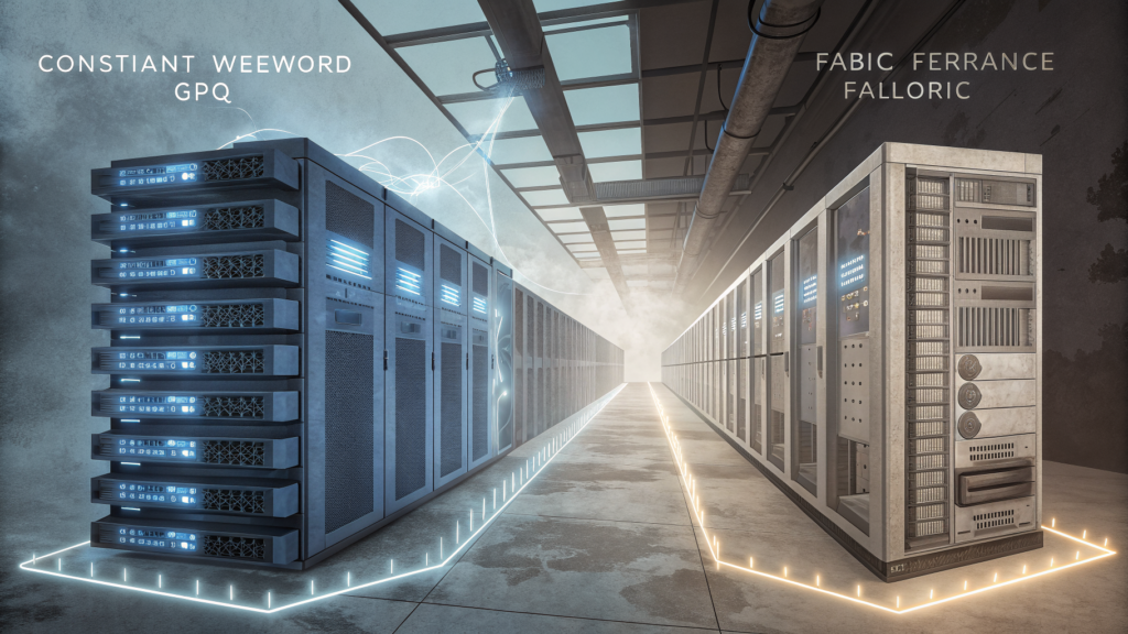
AMD’s play is more sophisticated than the acquisition framing suggests. The official press release describes integrating Taalas technology into AMD’s accelerator roadmap alongside Instinct GPUs, EPYC CPUs, and the ROCm software stack. The Register reported the specific architecture: AMD intends to split inference by phase, with Instinct GPUs handling prompt processing and Taalas chips handling token generation. Prefill on general-purpose compute. Decode on hardcoded silicon. This is not a bet against GPUs. It is an acknowledgment that prefill and decode have different resource profiles, and that the right architecture for a compute-bound problem is not the right architecture for a memory-bandwidth-bound problem. AMD is splitting the pipeline rather than unifying it under a single chip compromise.
The competitive context sharpens the strategy. Nvidia’s answer to the inference efficiency problem was to license Groq’s LPU architecture for $20 billion — a deterministic, low-latency processor that is still reprogrammable, still flexible, and does not solve the decode memory wall in the way Taalas does. The hyperscalers are building proprietary silicon with different constraints: Google’s Ironwood TPUs are vertically integrated into the pod; OpenAI is developing custom inference ASICs with Broadcom in a programmable architecture. MatX is building a programmable ASIC with on-chip SRAM that attacks the memory wall through bandwidth, not elimination — and has not yet shipped anything, with a 2027 target. Of all the inference chip bets on the table, Taalas is the most extreme: maximum efficiency through maximum inflexibility. AMD now holds it.
One detail about the Taalas team makes this acquisition more legible. Bajic co-founded Tenstorrent — a company building flexible, programmable AI accelerators that can run arbitrary models. He spent years working on the opposite of what Taalas built. He left and chose the hardest possible ASIC approach: one that cannot run anything except the model it was designed for. That is not ignorance of the tradeoffs. It is someone who understood the programmable design space well enough to conclude, deliberately, that certain workloads do not need flexibility and pay an enormous price for it. The HC2, planned for year-end 2026, will support larger parameter counts and pipeline parallelism across multiple cards, opening the architecture to frontier-class models for the first time. Taalas has been building toward that tier since the HC1 was a 25-employee beta.
AMD is now holding this bet. The HC1 runs on 6nm silicon, draws 200 watts per card, and serves Llama 3.1 8B at throughput that makes GPU-based decode look like the wrong tool for a job it inherited by default. The memory wall during token generation has always been inference’s most persistent structural constraint. Taalas solved it by making it physically nonexistent. The open question is whether AMD’s target customers — the inference providers running high-volume deployments of stable, proven models — are the ones whose workloads justify committing to dedicated silicon. If they are, this is the right architecture at the right moment in the market’s maturity. If production inference turns out to require more model diversity and faster iteration than Taalas’s economics assume, AMD bought an excellent answer to a question that only some of its customers are actually asking.
AI-generated editorial illustration · TemperatureZero · August 7, 2026
Keep reading the signal
Get the Daily Signal — a concise briefing on what actually matters in AI and the systems around it.
Subscribe FreeContinue the archive