On May 20, NVIDIA reported $81.6 billion in quarterly revenue — $75.2 billion of it from data center. Jensen Huang called the buildout “the largest infrastructure expansion in human history.” That quote got the coverage. What didn’t: a day later, Epoch AI published an analysis of what, exactly, is inside the chips driving that expansion. The headline finding is that high-bandwidth memory now accounts for 63% of total AI chip component spending — up from 52% in Q1 2024, a shift of eleven percentage points in twenty months. The logic die, the thing people point to when they call it a GPU, is 13%.
The AI hardware race is not a compute race. It’s a memory race. The press is covering the wrong variable.
The Math Inside the Machine
Venkat Somala’s analysis at Epoch AI tracks per-chip component costs across four categories: HBM stacks, advanced-node logic dies running at 3–5nm, TSMC’s CoWoS advanced packaging, and auxiliary components. The dataset draws on financial disclosures, supplier filings, and analyst reports across Nvidia, AMD, Google, and Amazon chip designs, weighted by production volume. It is the most granular public decomposition of AI chip economics available.
In Q1 2024, HBM accounted for 52% of total AI chip component spending. By Q4 2025, that share had risen to 63%, with a confidence range of 60–67%. The other buckets in Q4 2025: advanced packaging at 15%, auxiliary components at 10%, and logic dies at 13%. The compute — the 3nm silicon that does the matrix multiplications everyone talks about — is thirteen cents on the dollar.
The absolute numbers make this concrete. HBM spending grew from approximately $12 billion in 2024 to $32 billion in 2025, a $20 billion increase in a single year. Total AI chip component spending rose from $22 billion to $52 billion over the same period. Memory captured roughly two-thirds of that $30 billion increase. Advanced packaging grew from around $4 billion to roughly $8 billion. Logic dies — the actual compute — grew from around $3 billion to around $7 billion.
Epoch AI’s analysis finds that Microsoft raised its FY2026 capital expenditure outlook by $25 billion citing higher component prices, and Meta raised its 2026 capex guidance by $10 billion for the same reason. These are not expansionary moves driven by ordering more chips. They are cost-driven moves driven by the rising price of the memory inside the chips already ordered. The distinction matters. Microsoft isn’t adding 25% more capacity than originally planned. Microsoft is paying 25% more for the capacity it planned.

What 13.4 Terabytes Actually Means
NVIDIA’s GB200 NVL72 — the current flagship AI training rack — contains 13.4 terabytes of HBM3e memory across 72 Grace Blackwell Superchips. Aggregate memory bandwidth across the system is 576 terabytes per second. Each superchip carries 372 gigabytes of HBM3e at 16 terabytes per second of bandwidth; 72 of them connect via 130 terabytes per second of NVLink, allowing the full rack to function as a single logical GPU with 13.4 terabytes of addressable memory.
Micron, which now has HBM4 in high-volume production in a 36-gigabyte 12-layer configuration, rates its newest product at over 11 gigabits per second per pin, delivering more than 2.8 terabytes per second of bandwidth per stack. HBM4 delivers 2.3 times the bandwidth of HBM3e at 20% lower power consumption. Micron describes it as “the most complex memory design ever made.” That description is not marketing copy — it is a supply chain warning.
The reason memory commands 63% of chip cost is architectural, not incidental. Training large transformers at scale is not primarily compute-bound; it is memory-bandwidth-bound. Running a frontier model requires moving enormous weight tensors through cache repeatedly across each training step. The operation stalls waiting for data, not waiting for FLOPS. Every architectural choice that makes models more capable — more attention heads, longer context windows, larger batches — increases memory bandwidth pressure faster than it increases raw compute pressure. Attention is quadratic in sequence length; the memory required to hold the key-value cache at the frontier scales with it. The compute requirement grows, but the ratio keeps moving toward memory.
NVIDIA is not primarily selling compute. It is selling memory bandwidth at extraordinary density. The progression from H100 to B200 to the GB200 system is fundamentally a memory bandwidth roadmap. The H100 delivers 3.35 terabytes per second at 80 gigabytes of HBM2e. The B200 delivers 8 terabytes per second at 192 gigabytes of HBM3e. The GB200 NVL72 hits 576 terabytes per second in aggregate — roughly 172 times the bandwidth of a single H100, for a system that is, on raw FLOPS, perhaps 20–40 times more powerful. The FLOPS justify the purchase. The memory bandwidth is the product.
The pace of HBM improvement explains why this gap keeps widening. Epoch AI’s data insights series tracks aggregate AI chip memory bandwidth growing at 4.1x per year, now reaching 70 million terabytes per second across all deployed AI accelerators — a rate that far outpaces general DRAM improvements. LPDDR5X, which serves the CPU side of the GB200’s 17-terabyte CPU memory pool, delivers 14 terabytes per second for the entire 36-CPU array. A single B200 GPU’s HBM3e delivers 8 terabytes per second on its own. The bandwidth gap between general-purpose memory and HBM is not narrowing. It is the economic justification for the premium, and the premium keeps growing because the gap keeps growing.
Three Companies Own the Constraint
SK Hynix, Samsung, and Micron are the only manufacturers currently producing HBM at volume for AI accelerators. HBM manufacturing requires EUV lithography for the advanced nodes, combined with the through-silicon via stacking process that bonds multiple DRAM dies into a single high-density column. This is not the same manufacturing challenge as producing DRAM for consumer applications or NAND for SSDs — it is substantially more complex, and the process has been in development for a decade. SK Hynix received the 2026 IEEE Corporate Innovation Award specifically for driving AI computing expansion with HBM, recognition that underscores how thoroughly the company has made HBM its institutional identity. That decade of process refinement is the moat, and it is deepening every year.
The packaging constraint runs in parallel. CoWoS — TSMC’s Chip-on-Wafer-on-Substrate process — bonds HBM stacks to the logic die in AI accelerators. TSMC is the only volume producer of CoWoS at the node sizes required for B200 and GB200 chips. In 2025, CoWoS availability was itself a binding constraint: per Epoch AI’s analysis, HBM and advanced packaging together — not logic die production — were the primary limits on AI chip supply that year. The constraint is therefore two-layered: you need the memory, and you need the only foundry that can attach it. Both are effectively single-supplier situations at the frontier node.
This creates a structural oligopoly that the FLOPS conversation systematically obscures. There is no spot market for HBM. NVIDIA and AMD negotiate multi-year purchase agreements with the three manufacturers, and when allocation is tight — as it was through most of 2025 — smaller cloud providers and startups receive nothing. Not at higher prices. Not at all. The infrastructure gap between AWS, Azure, and Google Cloud on one side and everyone else is not a capital gap. It is a supply-access gap: the hyperscalers signed purchase agreements for memory that will not be on the open market for years.
The wildcard is ChangXin Memory Technologies, China’s state-backed DRAM producer. CXMT has reached volume production in DDR5 — Corsair recently shipped products using CXMT chips, which cleared quality testing for consumer applications. But HBM is a different manufacturing problem. HBM3 and HBM3e require EUV fabrication tools that export controls have kept out of CXMT’s fabs, and the through-silicon via stacking process is a separate challenge that CXMT has not demonstrated at volume. The gap between DDR5 production and HBM3e production is not a gap that closes in a fiscal year.
Whether that gap closes in three years or seven is the most consequential supply chain question in AI infrastructure. If CXMT reaches volume HBM production, the oligopoly breaks, prices normalize over a cycle, and the structural advantage held by hyperscalers with locked-in purchase agreements diminishes. If the EUV and TSV barriers hold through 2030, the infrastructure arms race plays out entirely inside the existing supply structure, and the companies that signed long-term HBM agreements in 2024 will have build-out capacity advantages that newcomers cannot buy their way into.
Microsoft and Meta did not raise their 2026 capex by a combined $35 billion because the models got better. They raised capex because the price of the memory inside their chips went up, and they need more of it. Huang’s “largest infrastructure expansion in human history” is real. It is also constrained by a packaging process at one Taiwanese foundry and a 12-layer stacked DRAM design that a handful of memory engineers have learned to produce reliably. The question that will determine who can build at the scale the next generation of AI models requires is not which lab has the best architecture. It’s which hyperscaler signed the right purchase agreement in 2024. The companies that did are running. The ones that didn’t are in the queue.

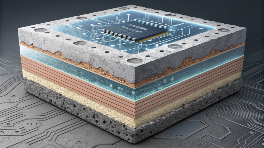
AI-generated editorial illustration · TemperatureZero · May 25, 2026
Keep reading the signal
Get the Daily Signal — a concise briefing on what actually matters in AI and the systems around it.
Subscribe FreeContinue the archive